- 您现在的位置:买卖IC网 > Sheet目录489 > NTLJD4150PTBG (ON Semiconductor)MOSFET P-CH DUAL 30V 3.2A 6WDFN
NTLJD4150P
Power MOSFET
?30 V, ?3.4 A, m Cool t Dual P?Channel,
2x2 mm WDFN Package
Features
? WDFN 2x2 mm Package Provides Exposed Drain Pad for
http://onsemi.com
?
?
?
?
Excellent Thermal Conduction
Footprint Same as SC?88 Package
Low Profile (< 0.8 mm) for Easy Fit in Thin Environments
Bidirectional Current Flow with Common Source Configuration
This is a Pb?Free Device
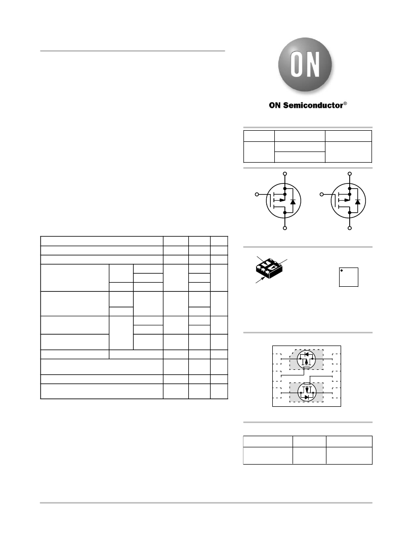
V (BR)DSS
?30 V
R DS(on) Max
135 m W @ 10 V
200 m W @ 4.5 V
S1
I D Max (Note 1)
?3.4 A
S2
Applications
? Li?Ion Battery Charging and Protection Circuits
? LED Backlight, Flashlight
? Dual?High Side Load Switch
MAXIMUM RATINGS (T J = 25 ° C unless otherwise noted)
G1
D1
G2
D2
Parameter
Symbol
Value
Unit
P?CHANNEL MOSFET
P?CHANNEL MOSFET
Drain?to?Source Voltage
Gate?to?Source Voltage
V DSS
V GS
?30
± 20
V
V
D2
D1
MARKING
DIAGRAM
G
Continuous Drain Current
(Note 1)
Steady
State
t ≤ 5s
T A = 25 ° C
T A = 85 ° C
T A = 25 ° C
I D
?2.7
?2.0
?3.4
A
Pin 1
WDFN6
CASE 506AN
1
2
3
JE M G 6
5
4
Power Dissipation
(Note 1)
Continuous Drain Current
(Note 2)
Power Dissipation
(Note 2)
Steady
State
t ≤ 5s
Steady
State
T A = 25 ° C
T A = 25 ° C
T A = 85 ° C
T A = 25 ° C
P D
I D
P D
1.5
2.3
?1.8
?1.4
0.7
W
A
W
JE = Specific Device Code
M = Date Code
G = Pb?Free Package
(Note: Microdot may be in either location)
PIN CONNECTIONS
Pulsed Drain Current t p = 10 m s
Operating Junction and Storage Temperature
I DM
T J ,
?14
?55 to
A
° C
S1
1
D1
6
D1
T STG
150
Source Current (Body Diode) (Note 2)
I S
?1.8
A
G1
2
5
G2
Lead Temperature for Soldering Purposes
(1/8 ″ from case for 10 s)
T L
260
° C
D2
3
D2
4
S2
Stresses exceeding Maximum Ratings may damage the device. Maximum
Ratings are stress ratings only. Functional operation above the Recommended
Operating Conditions is not implied. Extended exposure to stresses above the
Recommended Operating Conditions may affect device reliability.
1. Surface Mounted on FR4 Board using 1 in sq pad size (Cu area = 1.127 in sq
[2 oz] including traces).
(Top View)
ORDERING INFORMATION
2. Surface Mounted on FR4 Board using the minimum recommended pad size.
Device
NTLJD4150PTBG
Package
WDFN6
(Pb?Free)
Shipping ?
3000 / Tape &
Reel
?For information on tape and reel specifications,
including part orientation and tape sizes, please
refer to our Tape and Reel Packaging Specifications
Brochure, BRD8011/D
? Semiconductor Components Industries, LLC, 2007
January, 2007 ? Rev. 0
1
Publication Order Number:
NTLJD4150P/D
发布紧急采购,3分钟左右您将得到回复。
相关PDF资料
NTLJF3117PTAG
MOSFET P-CH 20V 2.3A 6-WDFN
NTLJF3118NTBG
MOSFET N-CH 20V 2.6A 6-WDFN
NTLJF4156NT1G
MOSFET N-CH 30V 2.5A 6-WDFN
NTLJS1102PTBG
MOSFET P-CH 8V 3.7A 6-WDFN
NTLJS2103PTAG
MOSFET P-CH 12V 3.5A 6-WDFN
NTLJS3113PTAG
MOSFET P-CH 20V 3.5A 6-WDFN
NTLJS3180PZTBG
MOSFET P-CH 20V 3.5A 6-WDFN
NTLJS4114NT1G
MOSFET N-CH 30V 3.6A 6-WDFN
相关代理商/技术参数
NTLJF117P
制造商:ONSEMI 制造商全称:ON Semiconductor 功能描述:High Efficiency DC-DC Converters
NTLJF156N
制造商:ONSEMI 制造商全称:ON Semiconductor 功能描述:High Efficiency DC-DC Converters
NTLJF3117P
制造商:ONSEMI 制造商全称:ON Semiconductor 功能描述:Typical Uses for FETKY Devices
NTLJF3117P_1
制造商:ONSEMI 制造商全称:ON Semiconductor 功能描述:Typical Uses for FETKY Devices
NTLJF3117PT1G
功能描述:MOSFET PFET 2X2 20V 4.1A 106MOHM RoHS:否 制造商:STMicroelectronics 晶体管极性:N-Channel 汲极/源极击穿电压:650 V 闸/源击穿电压:25 V 漏极连续电流:130 A 电阻汲极/源极 RDS(导通):0.014 Ohms 配置:Single 最大工作温度: 安装风格:Through Hole 封装 / 箱体:Max247 封装:Tube
NTLJF3117PTAG
功能描述:MOSFET PFET 20V 4.1A 106MO 2X2 RoHS:否 制造商:STMicroelectronics 晶体管极性:N-Channel 汲极/源极击穿电压:650 V 闸/源击穿电压:25 V 漏极连续电流:130 A 电阻汲极/源极 RDS(导通):0.014 Ohms 配置:Single 最大工作温度: 安装风格:Through Hole 封装 / 箱体:Max247 封装:Tube
NTLJF3118N
制造商:ONSEMI 制造商全称:ON Semiconductor 功能描述:Typical Uses for FETKY Devices
NTLJF3118NTAG
功能描述:MOSFET NFET 2X2 20V 3.8A 70MOHM RoHS:否 制造商:STMicroelectronics 晶体管极性:N-Channel 汲极/源极击穿电压:650 V 闸/源击穿电压:25 V 漏极连续电流:130 A 电阻汲极/源极 RDS(导通):0.014 Ohms 配置:Single 最大工作温度: 安装风格:Through Hole 封装 / 箱体:Max247 封装:Tube
